Creating a Parameterized Cell in Cadence
Often during circuit design, it is necessary to have multiple instances of a single cell (e.g., an inverter) but each instance may have different parameters (e.g., different transistor sizes). For example, consider the case where a circuit has a chain of inverters where each inverter has been scaled for minimum delay. One way in which this can be realized is to simply instance multiple transistors each having their own size. This is fine if there is only one such chain. If, however, multiple such inverter chains exist in a circuit is can be cumbersome if it is necessary to change one stage in the chain. This is especially true if the circuit is more complex than a simple chain of inverters.
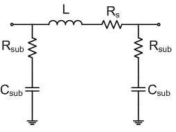
A better solution is to create a parameterized cell (p-cell). The p-cell can then be instanced and the parameters of interest individually set. Then if a circuit change within the p-cell is required, only one change must be made and it will automatically be reflected in all instances. This tutorial discusses how to create such a p-cell using a realistic inductor model as an example. The inductor model that we will be using is shown below:

where:
R_s = -0.0296*L^2 + 1.83*L + 2.288
C_sub = -0.0005*L^2 + 0.0312*L + 0.0543
R_sub = 0.0789*L + 31.707 + 3.4892/L
In the above equations, L is in nH, R_s and R_sub are in Ohms, and C_sub is in pF. In this case we want the value of inductance (in nH) to be in the form of a prameter.
- In order to create our p-cell we will take the following steps:
- Start Cadence and create a new cell view which we will call
ind_real. - Draw the schematic of the 9-element inductor model shown above
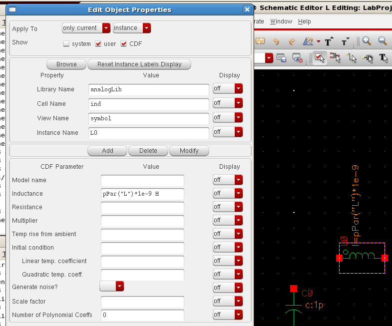
- Now select the inductor and press
qto view its properties. - Where you would normally set the value of inductance, enter the command:
pPar("L")*1e-9
This command tells Cadnece that we will have a parameter L that will be entered by the user upon instancing our newly created cell. We multiply this value by 1e-9 because according to the model above, L should be in nH.

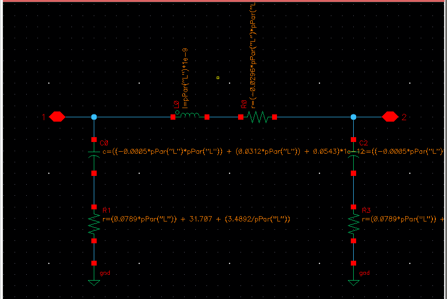
- Now in a similar fashion enter the equation for all of the remaining components and remember that the
pParcommand is case senstive. Also pay attention to the units of each part and make sure that they are defined properly.
- Add pins to port 1 and port 2 of the inductor in preparation for creating the symbol and then check and save your schematic. The resulting schematic should look like the following:
