Integrated Inductor Design using ADS Momentum: Difference between revisions
No edit summary |
No edit summary |
||
| (One intermediate revision by the same user not shown) | |||
| Line 34: | Line 34: | ||
*Create a new layout window by clicking <code>Window->New Layout</code> | *Create a new layout window by clicking <code>Window->New Layout</code> | ||
*You will now import the *.gds file that you created from your Cadence layout. In the ADS layout window click <code>File -> Import</code><br />[[Image:Import_ADS.png|center|border]]<br /> | *You will now import the *.gds file that you created from your Cadence layout. In the ADS layout window click <code>File -> Import</code><br />[[Image:Import_ADS.png|center|border]]<br /> | ||
**It is important to note that the above dialog box may be different depending on the version of ADS you are using. This is particularly for '''ADS 2012''. So although the following instruction may not be quite the same for your version, the idea will usually be the same. | **It is important to note that the above dialog box may be different depending on the version of '''ADS''' you are using. This is particularly for '''ADS 2012'''. So although the following instruction may not be quite the same for your version, the idea will usually be the same. | ||
**In the '''File Type''' select '''GDSII Stream Format''' | **In the '''File Type''' select '''GDSII Stream Format''' | ||
**Enter the name and location of your *.gds file in the '''Import file name (source)''' field or you can just browse to it, usually located in Cadence lunch directory. | **Enter the name and location of your *.gds file in the '''Import file name (source)''' field or you can just browse to it, usually located in Cadence lunch directory. | ||
| Line 40: | Line 40: | ||
**Load the same layer mapping file as in Cadence by clicking <code>Options->Layer</code> and select <code>Load custoum layer map file</code> on the drop down menu and load your cds2gds.map file. | **Load the same layer mapping file as in Cadence by clicking <code>Options->Layer</code> and select <code>Load custoum layer map file</code> on the drop down menu and load your cds2gds.map file. | ||
<br />[[Image:Map_ADS.png|center|border]]<br /> | <br />[[Image:Map_ADS.png|center|border]]<br /> | ||
*Click '''OK''' | |||
*Once you have imported your *.gds file into ADS you should see your inductor layout in the ADS layout window. Save your work, and remember that you must save the layout in the current project directory as this is where ADS will look for it. | *Once you have imported your *.gds file into ADS you should see your inductor layout in the ADS layout window. Save your work, and remember that you must save the layout in the current project directory as this is where ADS will look for it. | ||
**In general it is best to let ADS save the file in the default location. It causes fewer headaches later on. | **In general it is best to let ADS save the file in the default location. It causes fewer headaches later on. | ||
Latest revision as of 17:21, 5 June 2013
A common passive component in RFIC design is the integrated inductor and designers are commonly interested in the total inductance as well as the quality factor, or Q. In this tutorial you will learn how to take the layout of an inductor that was generated using Cadence and import it into ADS Momentum where you can find the inductance and Q values for that particular layout. This tutorial can also be adapted to designing integrated transformers where one is also interested in the coupling factor, k.
It is assumed that the reader is familiar with the basic operation of Cadence and the basic operation of ADS.
Inductor Layout
- Begin by starting Cadence and creating a new layout cell view for the inductor. It is important that each inductor be given its own cell view because we will later be generating a time-domain model for use in future Cadence simulations and this model will be specific to a particular layout.
- Once you have created the new layout view, click on
Options->Displayand change the X Snap Spacing and the Y Snap Spacing to the minimum spacing required by your fabrication process.- If you are using a Cadence Process Design Kit (PDK) this setting is likely to be set by default.
- Create the inductor layout making sure that it is DRC clean
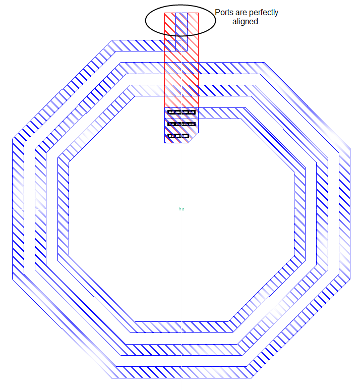
- IMPORTANT: It is imperative that the ports of the inductor are lined up exactly. If they are misaligned by even one grid spacing the resulting ADS simulations may become inacurate. In the below example the ports line up exactly in the y-dimension. The x-dimension does not matter (i.e., the ports do NOT have to be right on top of each other)
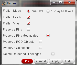
- If you instance a parameterized cell (p-cell) inductor, then you should flatten the layout by selecting
Edit->Hierarchy->Flatten. The following dialog box will open. It just give you some options on what you need to flatten. The default should just be fine. Click OK.
- IMPORTANT: It is imperative that the ports of the inductor are lined up exactly. If they are misaligned by even one grid spacing the resulting ADS simulations may become inacurate. In the below example the ports line up exactly in the y-dimension. The x-dimension does not matter (i.e., the ports do NOT have to be right on top of each other)
- Now that the layout is flatten, delete everything but the drawing layers from the design.If you are using the IBM PDK, make sure the following layers are preserved: MA, F1, E1, FT,and LY Drawing,F1 and FT BAR, the contact between MA and E1 and E1 and LY respectively.
Exporting Layout to ADS
We will now export the inductor layout to a *.gds file in preparation for simulation and modeling of the inductor in ADS Momentum.
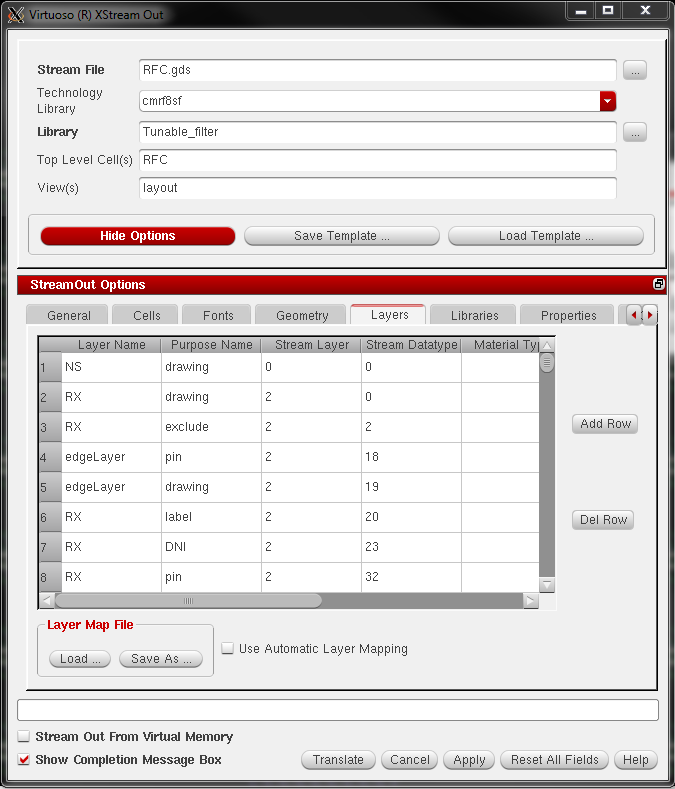
- In the Cadence CIW window click
File->Export->Streamthis brings up the Stream Out window.- Enter the name of the exported gds file. The file should have an extension '.gds' in the Stream File field.
- In the Technology Library field, enter the technology library that is attached to your working library. This will often be the name of your Cadence PDK library.
- In the Library field, enter the name of the Library where the inductor cell view is located
- In the Toplevel Cell(s) field, enter the name of the cell view containing the inductor layout
- In the View field enter the view name of the inductor layout (e.g., layout)
- Select Show Options and then the Layers tab
- Click on Load File and load the layer mapping file (if you have one). This file maps the cadence layers (i.e., M1, V12, M2, etc.) to gds layers and will have an extension of *.map. It may be called something like cds2gds.map and if you are using a PDK this file will sometimes be included in the PDK files. You can also use Automatic Mapping if no mapping file exists.
- In the Stream Out window click Translate. Make sure there are not errors. The warning can be ignored for the time being.
ADS S-Parameter Simulation
ADS is a 2.5-D electromagnetic simulator. You will use ADS to perform S-parameter simulations on your inductor layout and then extract characteristics such as inductance, quality factor, and self-resonant frequency from the results. Typically, the inductor is being designed for use in a larger circuit that will be designed using Cadence. You can also use ADS to generate an equivalent time-domain model of the inductor for use in future Cadence simulations. This process will be broken up into several steps and it is assumed that the reader has some basic familiarity with ADS.
Importing the Layout into ADS
- Begin by starting ADS and creating a new project. Alternatively, you can open an existing project.
- Create a new layout window by clicking
Window->New Layout - You will now import the *.gds file that you created from your Cadence layout. In the ADS layout window click
File -> Import
- It is important to note that the above dialog box may be different depending on the version of ADS you are using. This is particularly for ADS 2012. So although the following instruction may not be quite the same for your version, the idea will usually be the same.
- In the File Type select GDSII Stream Format
- Enter the name and location of your *.gds file in the Import file name (source) field or you can just browse to it, usually located in Cadence lunch directory.
- In the Layers file name enter the name of the ADS layers file (if one exists). If you are using a PDK it is likely that such a file (with file extension *.lay) exists in the PDK files. If one does not exist, you can create one by hand or simply leave the field blank.
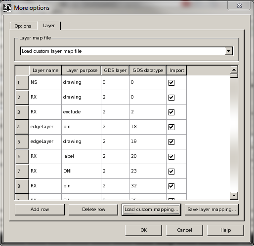
- Load the same layer mapping file as in Cadence by clicking
Options->Layerand selectLoad custoum layer map fileon the drop down menu and load your cds2gds.map file.
- Click OK
- Once you have imported your *.gds file into ADS you should see your inductor layout in the ADS layout window. Save your work, and remember that you must save the layout in the current project directory as this is where ADS will look for it.
- In general it is best to let ADS save the file in the default location. It causes fewer headaches later on.
- We must make sure that the ADS grid spacing matches the grid spacing used in Cadence to create the layout. In the layout window click
Options->Preferencesand click on the Grid/Snap tab - Change the Snap Grid Distance (in layout units) to match the X Snap Spacing and Y Snap Spacing that was used in Cadence
- You can leave the Snap Grid Per Minor Display Grid and the Snap Grid Per Major Display Grid at the default values
- It is a good idea to merge all of the metal layers as this will help speed up the simulation time
- This is done by selecting everything on one layer and clicking
Edit -> Merge -> Union - Repeat this step for each layer
- This is done by selecting everything on one layer and clicking
- Next you must insert ports. Click
Insert -> Pin - Place a port at each terminal of the inductor ensuring that the layer on which the port is inserted matches the metal layer on the inductor to which the port is being connected. Using
EM -> Pin -> Editoror by double clicking each port, make sure that all ports are with the impedance set to 50 Ohm- IMPORTANT: If the ports are on the same side of the inductor (see the figure below) the ports must be at exactly the same y-dimension for accurate simulation results.
- Snapping options exist for ease of placement
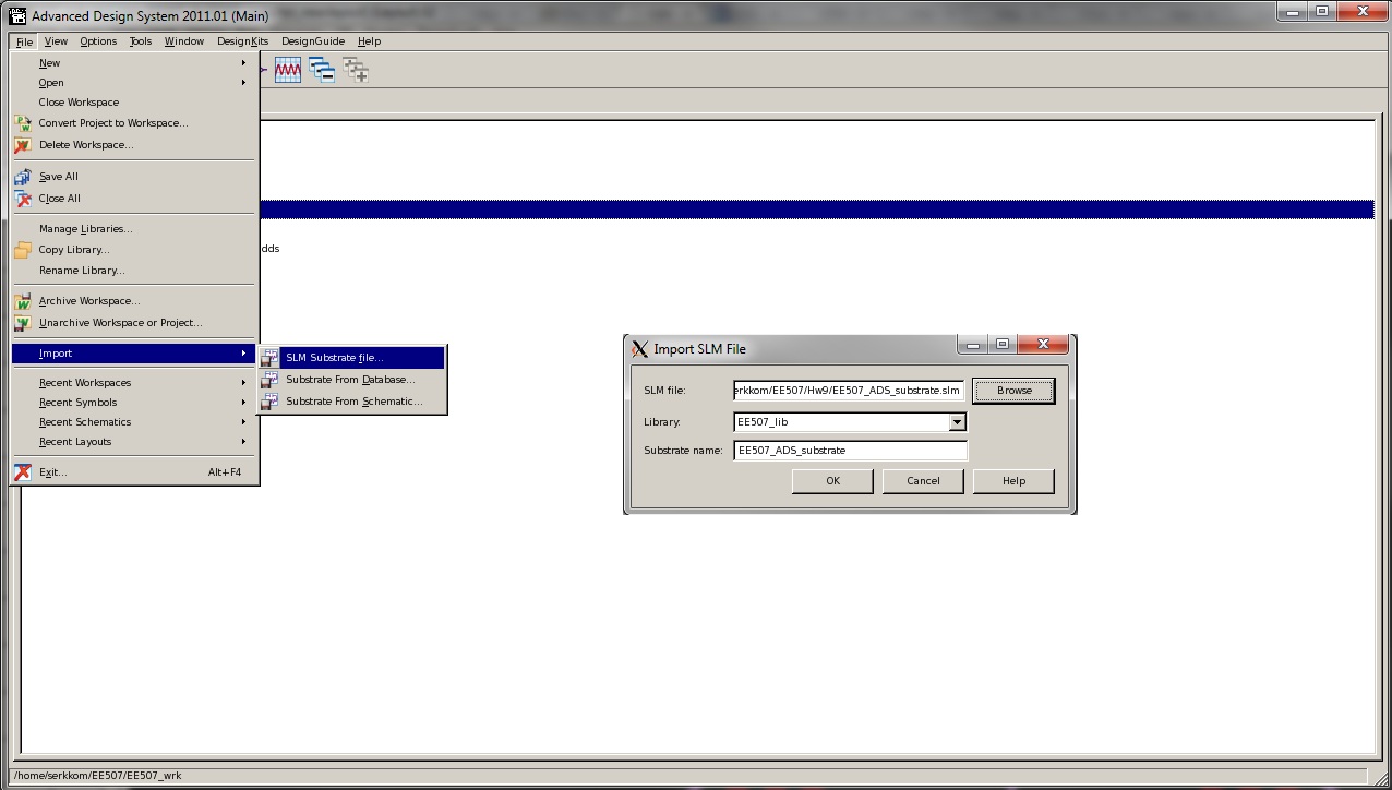
- Optional: import the substrate file if it has not been imported yet (e.g. you are using the substrate file for the first time)
Import the substrate file by going to the main windows of your ADS section and browse to your substrate file as shown below
Configure Simulation Settings
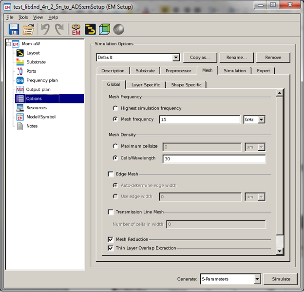
- The next step is to configure the Mesh. ADS uses the finite element method (FEM) to solve the complex differential equations required in order to get a solution for the EM fields generated by the structure of interest (in this case in inductor). As such it will generate a trapazoidal mesh and we need to define some of the characteristics of this mesh.
- Click
Substrateand make sure that your substrate file is displayed.- In the layout window click
EM->Mesh->Simulation Setup. The following windows will open.
- In the layout window click
- In
Options, underMeshtab, set the Mesh Frequency to a frequency higher than the maximum frequency of interest. For example if you wanted to model and inductor from 1 GHz to 10 GHz you might set the Mesh Frequency to 15 GHz - Set the Mesh Density to 30 cells/wavelength. The larger this number the more accurate the simulation but the longer the overall simulation time.
- Unselect Edge Mesh
- In
- You must now setup the S-parameter simulation
- Click
Frequency Plan - Fill in the Start and Stop frequencies and use the default values for everything else
- You can specify the name of the resulting dataset in the Dataset field
- Click Simulate
Note: that the first time you run the simulation it will take quite a long time because ADS must first generate the Green's functions and then save them. Subsequent simulations, however, will be much shorter because ADS will be able to simply load the precalculated Green's functions. The exception is if the simulation frequency range is increased. In this case ADS must recalculate the Green's functions for the new, expanded frequency range and hence the simulation will again take a long time. If the frequency range is reduced, this does not apply.
Viewing Results
You can now view the results, either as s-parameters or z- or y-parameters. From here you should be able to extract the inductance, Q, and self-resonant frequency.
Generating the Time-Domain Model
This section will deal with how to create a time-domain model that is equivalent to the layout that was simulated above. For this section you will need to have a dataset containing the S-parameter simulation results. This is obtained by simply running an S-parameter simulation over the frequency range of interest.
- Begin by creating a new schematic and build the inductor model of choice using ideal elements from the Lumped Components library. A common model is the 9-element model shown below where Ls is the series inductance, Rs is the series resistance, Cbr is the interwinding capacitance, Cox is the oxide capacitance, Csub and Rsub are used to model the effects of the lossy substrate.

- From the Data Items library add a data block with the same number of ports as your inductor.
- This is likely going to be 2, so you would add an s2p block. It could, however, be three if you are modeling a center tapped inductor or even more than four if you are modeling a transformer.
- Double click on the newly placed data item in your schematic to edit its properties.
- Make sure that under Parameter Entry Mode it reads Network parameter filename
- Under File Name enter the name of the dataset from your S-parameter simulation. The file extension should be a *.ds. (There will be two version of your dataset file dataset.ds and dataset_a.ds. You should choose the dataset_a.ds)
- Under File Type select Dataset
- You must now add ports to your schematic. These are found under the Simulation-S_Param library and they are called Term
- Place ports on both the time-domain model and the N-port data item. It is important that you correlate the port numbers on your model to the port numbers in your layout!
- From this same library also place a SP block. This is how you define the type of simulation to run in ADS and this block tells ADS to run an s-parameter simulation.
- Set the start and stop frequencies to the range over which you want to model the inductor. Remember that the maximum range is the range used in the layout s-parameter simulations.
Now the process involves changing the component values of the model until the model s-parameters match the s-parameters obtained from the layout simulations (represented here as the N-port data item). This can be a tedious process and so we will use the ADS optimization tool.
Optimization Tool
- Two items must be placed on the schematic in order to make use of the optimization tool
- The Optim block from the Optim/Stat/Yield/DOE library
- The required number of goal function blocks also from the Optim/Stat/Yield/DOE library.
- The number of goal functions will depend on the number of ports you have in your model. In general you will have two goal functions for each S-parameter you need to match. For example, assume that you are modeling a 2-port inductor you will need eight goal functions; two to optimize magnitude and phase of S11, two to optimize magnitude and phase of S12, two to optimize magnitude and phase of S21, and two to optimize magnitude and phase of S22.
- Set the goal functions to minimize the difference between Sij of the model and Sij of the N-port data item.
- Double click on the optimizer (the Optim block placed earlier) and choose the type of optimization that you would like to run.
- A good approach is to start with random in order to get close to a solution and then use derivative in order to drive the solution to a local minimum.
- When everything is configured, click
Simulate->Runor click the run icon in the schematic window - When the simulation is over, the results file will open up. Examine the S-parameters of the model and compare them to the S-parameters of the N-port data item (i.e., the layout). You will notice that as you run the optimizer the results become very close meaning that your model is doing a good job of modeling the layout. You will keep iterating with the optimizer until you have a model with the required accuracy.
- You can update the schematic with the optimized values by clicking
Simulation->Update optimization valuesin the schematic window. - Keep in mind that this is a relatively simple model and while it will likely provide a good match from 1 GHz to 10 GHz it will start to loose accuracy beyond thos values and you may need to use a more complex model to get the desired level of wideband matching.
- You can update the schematic with the optimized values by clicking
- Once you have a model that gives you the required accuracy, create a new schematic in cadence and copy the component values. You now have a time-domain model for use in Cadence simulations.