Simulations using ADE (G)XL: Difference between revisions
Jump to navigation
Jump to search
| (11 intermediate revisions by the same user not shown) | |||
| Line 62: | Line 62: | ||
*[[MonteCarlo Simulations using ADE XL]] - Monte Carlo simulations using ADE XL in Cadence | *[[MonteCarlo Simulations using ADE XL]] - Monte Carlo simulations using ADE XL in Cadence | ||
==Parasitic Extraction== | |||
*DRC | |||
**For the purpose of this tutorial, we will use a simple inverter schematic and layout. | |||
**So the first thing is to design your circuit and the corresponding layout. | |||
**On the layout we want to make sure that no design rules are violated by using the DRC(Design Rules Checker) tool of the PDK. | |||
**On the layout windows, go to <code>IBM_PDK --> Checking --> Assura --> DRC</code> as shown below. | |||
[[Image:DRC.png|center|border]] | |||
*A new dialogue box '''Run Assura DRC''' will open as seen below on top left. | |||
**Make sure it is pointing to your layout | |||
**The run name can be anything you choose but make sure that your '''Run Directory''' is set to some newly created directory otherwise there will be a lot of unwanted file in your cadence home directory. In my case I created a directory called '''DRC_LVS''' where all the trash file will go after each run. | |||
**We also need to tell cadence what design rule to use when checking our design which is usually located in the '''PDK''' directory under '''.../relDM/Assura/DRC/drc.rul'''. | |||
**It is also important to set the switches as shown on the left side of the the image below in order for cadence to correctly run the DRC rule we provided. | |||
**After setting everything as described above, click OK and DRC will run and the output will be shown as the '''Error layer Windows''' on the bottom part of the image above. You are DRC clean if all that are displayed are '''#INFO'''. Otherwise fix any type of errors before moving forward by using the '''AV/NV''' that will help you locate the error area on your layout. | |||
[[Image:DRC_Setup.png|center|border]] | |||
*LVS | |||
**Now that we are DRC clean we will compare our schematic and layout by running LVS(Layout Vs Schematic) | |||
**Go to <code>IBM_PDK --> Checking --> Assura --> LVS (VLDB)</code> as shown below. | |||
**'''Run Assura LVS''' Dialog box will open. | |||
**Browse to your schematic and layout in their respective '''Design Source''' field. | |||
**Same consideration is needed for the '''Run Directory'''. The '''Run Name''' is not very important. | |||
**In the '''Extract Rules''' field browse to the '''extract32.rul''' file and pay attention to the '''32''' and it comes by default as '''323'''. You need to delete the '''3''' at the end. | |||
**No need to set the switches in this case. | |||
**If the '''Binding Files''' and the '''RSF Include''' are not set by default, set them as shown on the figure. | |||
**Click '''OK''' to run LVS | |||
**You should expect rthe following dialog box with no LVS issue. Otherwise there are mismatches that need to be resolved before moving forward. | |||
[[Image:LVS.png|center|border]] | |||
*QRC Extraction | |||
**The next step after DRC and LVS clean layout is the parasitic extraction that are not taken into account in schematic simulation | |||
**Go to <code>Assura --> Run QRC</code> | |||
**'''QRC(Assura)Parasitic Extraction Run Form''' will open. | |||
**Under '''Setup''' tab, change the '''Output''' to '''Extracted View''' as shown below. | |||
** Click '''OK''' | |||
[[Image:QRC_Setup.png|center|border]] | |||
[[Image:LVS_Setup.png|center|border]] | |||
*Extracted Layout | |||
**Go to your cadence '''Library Manager''' and under the view of your design you should see a new view called '''av_extracted''' which is the result of the above '''QRC''' extraction. | |||
**When you open it, is will look something similar to the following. This will be what cadence will use for post layout parasitic simulation. '''Alway make sure your top level symbol descends to this view when you intends to run post layout simulation otherwise your results might be a little too optimistic'''. | |||
[[Image:Extracted_View.png|center|border]] | |||
==Postlayout simulation== | ==Postlayout simulation== | ||
*Create a test in ADE (G)XL using schematicview | *Create a test in ADE (G)XL using schematicview | ||
[[Image:TB.png|center|border]] | |||
*Setup the simulation configurations (or, you can setup the simulation configurations for schematic view in ADE L and save the state. Load the saved state). | *Setup the simulation configurations (or, you can setup the simulation configurations for schematic view in ADE L and save the state. Load the saved state). | ||
*Setup the extract view: parasitics>setup>choose the cell to setup its schematic, estimated, an extracted view | *Setup the extract view: parasitics>setup>choose the cell to setup its schematic, estimated, an extracted view | ||
[[Image:Parasitic.png|center|border]] | |||
*Run the simulation | *Run the simulation | ||
**No parasitic: schematic simulation | **No parasitic: schematic simulation | ||
**Extracted: postlayout simulation | **Extracted: postlayout simulation | ||
[[Image:Graph.png|center|border]] | |||
Latest revision as of 18:15, 12 June 2013
Setups for proper usage of ADE XL for NCSU CDK
- Edit .cdsenv in the project library, add the following lines
; To run adexl properly for NCSU PDK
adexl.icrpStartup  binaryName string "virtuoso -nocdsinit"
Simulations using ADE (G)XL
- First you need to create a test using the config view because Test using schematic view can be only used for schematic simulation. It is highly recommended to create a test using config view, which can be conveniently used for both schematic and postlayout simulation. The procedure is the same as a new schematic creation procedure except that the view needs to be config as shown below.

- In the New Configuration windows that opens, shown on the right side of the above image. For the template, we want to use spectre by clicking on
Use Templateand choosing spectre. Then set your top cell accordingly. - Now that we have our test setup, we will create a new ADE (G)XL by going to
Launch--> ADE XLin your config test windows. You will have the choice to create a new view or open and existing view. Here we will just use the default as shown below.
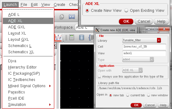
- In the Create new ADE(G)XL view dialog box that opened change the view type to adexl and make sure that Cell corresponds to your design top level test bench as shown above.
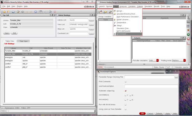
- Now you should have setup as shown below. Here it is important to make sure that the of your top level or any lower hierarchy is set to schematic when you want to run a schematic simulation or av_extracted in case you want to run a layout extracted view of that particular level. Also look at the environment under setup in your ADE windows to make sure that the view you intended to simulate is displayed first in the Parameter Range Checking File box. Otherwise you may be misled in your simulation which can be costly.
Parameter sweeping
- Option 1
- Double click the parameter value
- Click the button on the right of the value
- Run simulation
- Option 2
- Setup the parameter sweep in ADE L
- Save the setup to an .il file
- Load the saved .il file into ADE (G)XL parameter setup
- Run simulation
Corner Simulations using ADE XL
- Corner Simulations using ADE XL - Corner simulations using ADE XL in Cadence
- Select Launch tab in the schematic.
- Select ADE XL.
- Select Create New View and then OK.
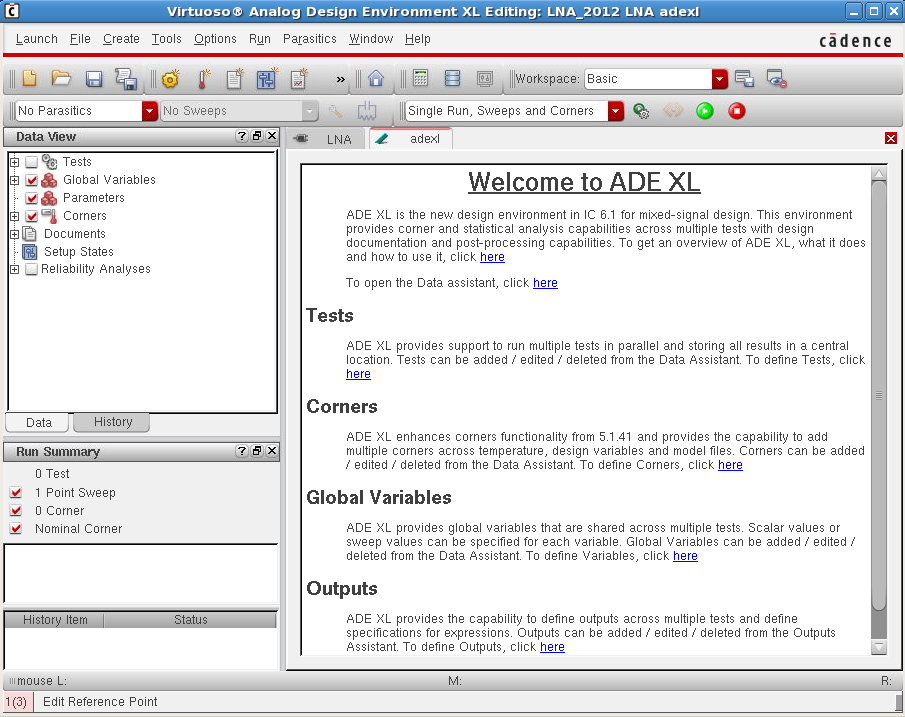
- Once you have created a new ADE XL window view, go to the
Data Viewwindow and select Tests.- Clcik Add Test.
- Setup the tests, model files, variables and outputs in the ADE L window.
- Added tests (etc.) should appear under Tests in
Data Viewwindow.
- In the
Data Viewwindow, select Corners.- Click Add Corner.
- Click Add Model File.
- Click Import from Test.
- Add other model files if needed.
- Click Add new corner.
- Click section and set the desired corner for the model files.
- Rename the added test to match corner simulation (Optional).
- Repeat the above for all corner tests.
- Click OK.
- Added corners should appear under Corners in
Data Viewwindow.
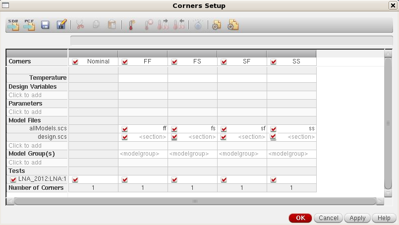
Note: You need to select the models that you are going to use by checking the corresponding box in the column of the corner.
- Run the simulation.
- To plot the results:
- Right click on graph symbol corresponding to the parameter you wish to plot.
- Select Plot Across Corners.
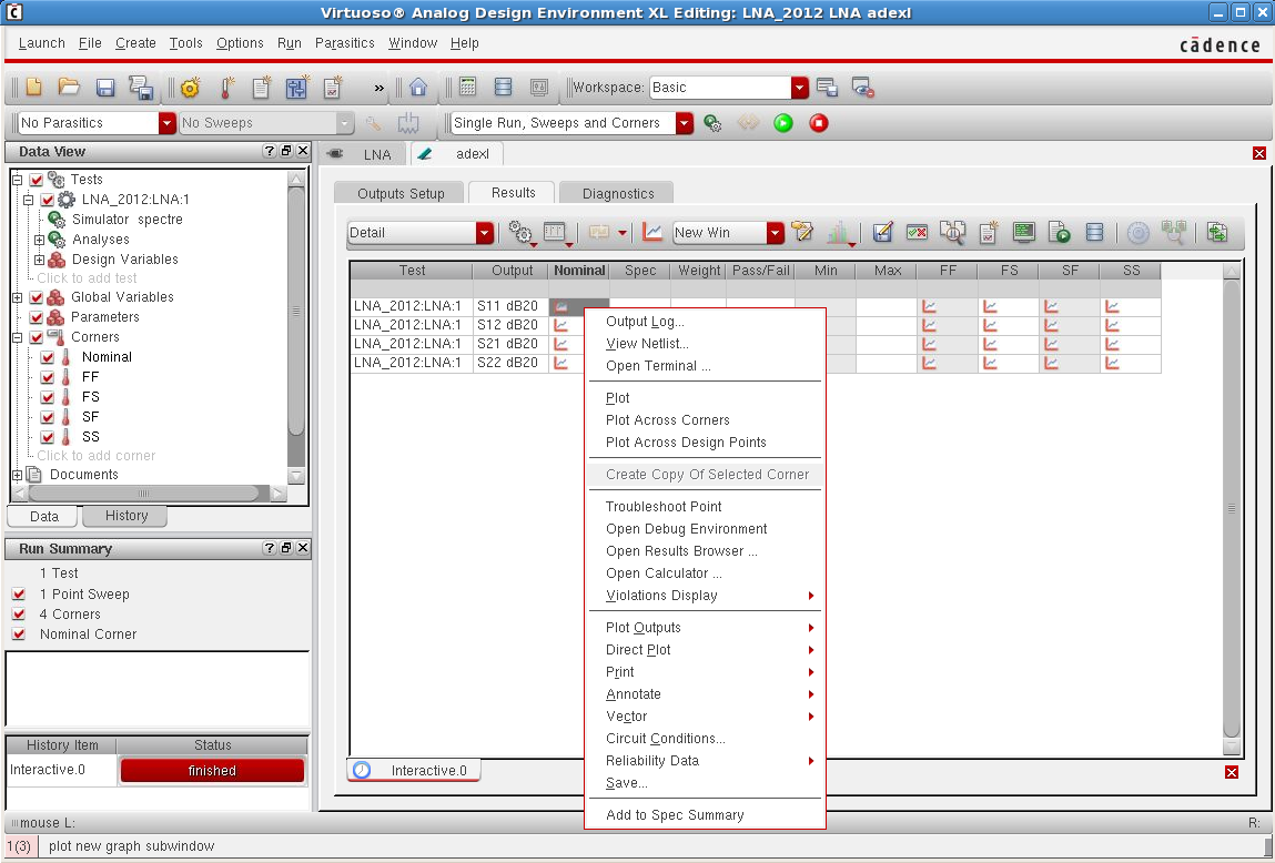
MonteCarlo Simulations using ADE XL
- MonteCarlo Simulations using ADE XL - Monte Carlo simulations using ADE XL in Cadence
Parasitic Extraction
- DRC
- For the purpose of this tutorial, we will use a simple inverter schematic and layout.
- So the first thing is to design your circuit and the corresponding layout.
- On the layout we want to make sure that no design rules are violated by using the DRC(Design Rules Checker) tool of the PDK.
- On the layout windows, go to
IBM_PDK --> Checking --> Assura --> DRCas shown below.

- A new dialogue box Run Assura DRC will open as seen below on top left.
- Make sure it is pointing to your layout
- The run name can be anything you choose but make sure that your Run Directory is set to some newly created directory otherwise there will be a lot of unwanted file in your cadence home directory. In my case I created a directory called DRC_LVS where all the trash file will go after each run.
- We also need to tell cadence what design rule to use when checking our design which is usually located in the PDK directory under .../relDM/Assura/DRC/drc.rul.
- It is also important to set the switches as shown on the left side of the the image below in order for cadence to correctly run the DRC rule we provided.
- After setting everything as described above, click OK and DRC will run and the output will be shown as the Error layer Windows on the bottom part of the image above. You are DRC clean if all that are displayed are #INFO. Otherwise fix any type of errors before moving forward by using the AV/NV that will help you locate the error area on your layout.

- LVS
- Now that we are DRC clean we will compare our schematic and layout by running LVS(Layout Vs Schematic)
- Go to
IBM_PDK --> Checking --> Assura --> LVS (VLDB)as shown below. - Run Assura LVS Dialog box will open.
- Browse to your schematic and layout in their respective Design Source field.
- Same consideration is needed for the Run Directory. The Run Name is not very important.
- In the Extract Rules field browse to the extract32.rul file and pay attention to the 32 and it comes by default as 323. You need to delete the 3 at the end.
- No need to set the switches in this case.
- If the Binding Files and the RSF Include are not set by default, set them as shown on the figure.
- Click OK to run LVS
- You should expect rthe following dialog box with no LVS issue. Otherwise there are mismatches that need to be resolved before moving forward.

- QRC Extraction
- The next step after DRC and LVS clean layout is the parasitic extraction that are not taken into account in schematic simulation
- Go to
Assura --> Run QRC - QRC(Assura)Parasitic Extraction Run Form will open.
- Under Setup tab, change the Output to Extracted View as shown below.
- Click OK


- Extracted Layout
- Go to your cadence Library Manager and under the view of your design you should see a new view called av_extracted which is the result of the above QRC extraction.
- When you open it, is will look something similar to the following. This will be what cadence will use for post layout parasitic simulation. Alway make sure your top level symbol descends to this view when you intends to run post layout simulation otherwise your results might be a little too optimistic.

Postlayout simulation
- Create a test in ADE (G)XL using schematicview

- Setup the simulation configurations (or, you can setup the simulation configurations for schematic view in ADE L and save the state. Load the saved state).
- Setup the extract view: parasitics>setup>choose the cell to setup its schematic, estimated, an extracted view

- Run the simulation
- No parasitic: schematic simulation
- Extracted: postlayout simulation
